In order to accurately emulate cycle-counted demo effects such as the Kefrens bars effect in 8088MPH, or the end credits in Area 5150, there are essentially four prerequisites:
- Cycle-accurate 8088 CPU emulation including processor instruction queue emulation
- Cycle-accurate CGA CRTC emulation
- Accurate DMA emulation for DRAM refresh
- Accurate CGA wait state emulation
This article will discuss the last item, CGA wait state emulation.
ISA Peripherals and I/O CH RDY
The number of wait states that the CPU inserts on each access to the CGA memory depends on the amount of time that the CGA card suppresses the I/O CH RDY signal, which is on ISA bus pin A10.
 |
ISA bus pinout, courtesy Wikipedia
|
This signal reaches the motherboard and is passed through miscellaneous TTL logic (on Sheet 2 of the Technical Reference) to eventually connect to the RDY pin on the 8284 clock generator, which in turn produces the READY signal to the CPU.
When READY is low during T3 of a bus transfer, the CPU inserts wait states until READY goes high.
In this manner, READY can be suppressed by both memory access and device IO, so wait states can be encountered during 'MOV' and string operations as well as IN and OUT.
The IBM PC and XT motherboards enforce a common minimum of a single wait state on all IO operations.
The CGA Wait States
Some devices, such as RAM or ROM chips, may have a rated response time in nanoseconds. They will require the same number of wait states (or none) each time they are accessed. This is fairly straightforward to emulate.
The CGA is not like this. Its wait time is variable, representing different wait periods depending on exactly when it is accessed. This makes emulating it a bit trickier.
Before continuing, I would recommend you read this blog post on the topic by reenigne, and the units he defines therein.
In this article reenigne describes the CGA wait state algorithm as follows:
The wait state algorithm for the original IBM CGA is basically "wait 1 hchar, then wait for the next lchar, then wait for the next ccycle"
This is interesting, but I wanted to know more. How exactly is this algorithm derived?
Fortunately, the situation turned out a bit simpler than I anticipated.
I/O CH RDY on the CGA
To begin our investigation then we must trace the logic that controls I/O CH RDY output on the IBM CGA. Fortunately, just like the motherboard schematics, IBM was kind enough to publish a full schematic of the CGA card in publication 6361509, "IBM Color/Graphics Monitor Adapter".
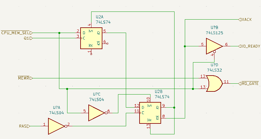
I/O CH RDY is found on the right side of Sheet 4 as "IO_READY"
Don't panic, much of this diagram can be ignored. I've transcribed the relevant portion for us:
IO_READY derivation, Sheet 4
That's a bit better. We can see that it relies on only a few signals for its calculation: !CPU_MEM_SEL, Q1, and RAS. There are two flip-flops in the picture, this effectively gates !CPU_MEM_SEL by Q1 and !RAS in turn, a combination of two signals that results in IO_READY directly, with a little logic to reset the signal when !CP_MEM_SEL is de-asserted.
Let's cover each of these input signals one at a time.
CPU_MEM_SEL
 |
| CPU_MEM_SEL derivation, Sheet 3. |
CPU_MEM_SEL itself is derived from a number of input signals, five lines from the address bus and two bus signals, !MEMR and !MEMW. The chip used is a 74LS138 demultiplexer, of which only a single output line is tied. The logic is fairly simple. The demultiplexer will take an binary input on its A0-A2 lines and raise the output of the decimal output pin corresponding to that value. In this case, since only O7 is tied, we will only match the situation where A15, A16, and A17 are all 1, or the addresses 11 1000 0000 0000 0000 - 11 1111 1111 1111 1111. But the output signal can also be suppressed by three enable lines, E1-E3. Two additional address lines are tied here. Note that two of these are inverted and one (E3) is not.
Adding in the logic for these two extra address lines, the final matching addresses are 1011 1000 0000 0000 0000 - 1011 1111 1111 1111 1111, or hex 0xB8000 - 0xBFFFF. You may recognize the base address of the CGA adapter at this point. Notice that since A14 is not decoded, the CGA will respond to the entire 32KB memory range, despite only having 16KB of video memory. This causes a mirroring of the CGA video memory at 0xBC000.
So CPU_MEM_SEL is asserted if either !MEMR or !MEMW are active and the CPU is accessing the CGA's defined memory range. Simple enough!
Q1 and RAS
The other two signals will be a little trickier. They are derived from the main 14Mhz system clock.
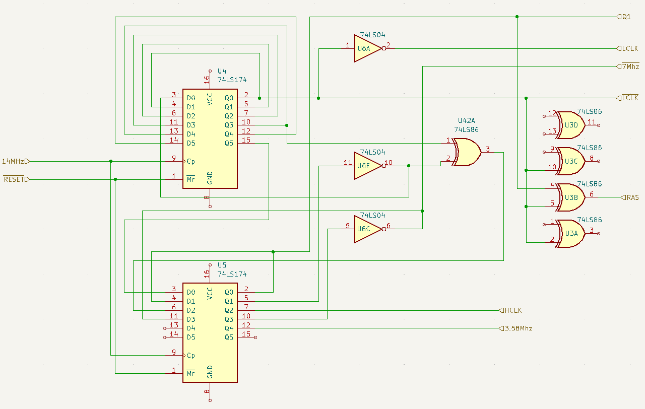
The CGA card takes this input clock and derives multiple different clocks of different periods and phases. The clock derivation circuitry is on Sheet 3:
Again I have transcribed the relevant portion for clarity:
 |
| CGA Miscellaneous Clock Derivation, Sheet 3 |
The 14Mhz system clock enters from the left into two connected flip-flops. You may notice that the outputs of the first flip-flop feed back into its own inputs, as well the first two outputs of the second flip-flop. We need an initiating high signal somewhere or all these inputs will stay 0. This provided by the inverter of U6E in the middle of the diagram, which in the initial state will place a high signal on the first input of the first flip-flop, D0.
It's not necessary to describe the function of these flip-flops in exhaustive detail - the six outputs of the first flip-flop combined with the first two outputs of the second flip-flop create 8 separate clock dividers at different phases which generate all the miscellaneous clocks the card requires.
One of our signals of interest, Q1, is taken off the first output of the second flip-flop. (Q0 on the diagram due to differences between KiCad and IBM's numbering). This divisor is effectively delayed by 6 system clocks, with the first flip-flop providing delays 0-5. I've done the work to decode all the relative clocks produced by this circuit:
 |
| CGA Clocks |
CPU cycles are provided at the top just for reference.
Notice !LCLK is the first output of our flip-flop so has no phase offset, and represents 16 system clocks. This is the low resolution character clock, used by the CGA in 40 column and low-resolution graphics modes. Additional divisor logic is used to produce the 8-tick HCLK, the high resolution character clock that we are more familiar with in 80 column modes.
Our second signal of interest, RAS, is also derived here, via a XOR gate connected to LCLK and Q1, !RAS becoming the product of those two clock's overlap.
Putting it Together
Let's look again at the IO_READY generator:
The first flip-flop receives !CPU_MEM_SEL as data, clocked by Q1. That means that !CPU_MEM_SEL will not be recognized until a low-to-high transition of Q1, which we know operates on a 16-cycle phase, with a 6-cycle phase offset.
Once this occurs, the output of the first-flip flop is high and proceeds to the second-flip flop, which is clocked on !RAS (note the inverter). !RAS is a periodic signal that goes high every 8 system clocks. The output of this second flip-flop is used as its own reset, which limits the time that IO_READY will be high.
One important thing to note is that the delays involved here mean that if Q1 and !RAS are both transitioning high in a single instant, the output of the first flip-flop is too late to be gated by the second - we must wait for the next transition of !RAS.
So our logic becomes:
- On a memory access, we must wait for the rising edge of Q1.
- We must them wait for the next rising edge of !RAS.
Q1 and RAS together produce a cycle that repeats every 16 system clocks, therefore this logic repeats every 16 system clocks. The CPU is not synchronized with the CGA card, so it can begin a read or write on any single one of those 16 clocks. This produces the 16 different wait states that reenigne mentioned.
 |
| System clock waits until IO_READY |
If a CPU access begins on Clock #0, we wait six system clocks for Q1. Note that there are 3 system clocks for each CPU cycle, so effectively we wait two CPU cycles. Q1 transitions high, latching the first flip-flop, but we're too late to latch on !RAS so we wait an additional 8 system cycles until !RAS goes high again until IO_READY is finally asserted, for a total of 14 system cycles of wait.
This wait decreases as CPU access occurs closer and closer to Q1, until it occurs on the same cycle that Q1 goes high. This is too late - so we must wait for the next Q1, which causes a jump or discontinuity in our nice orderly wait timing.
Therefore the possible waits are 14, 13, 12, 11, 10, 9, 24, 23, 22, 21, 20, 19, 18, 17, 16, and 15 system ticks for each of the 16 relative phases. We can convert these system ticks of delay into CPU cycles by dividing the CPU's clock divisor of 3 (14.138Mhz/3=4.77) and rounding upwards to the nearest integer, since the CPU cannot insert fractional wait states. This gives us 5, 5, 4, 4, 4, 3, 8, 8, 8, 7, 7, 7, 6, 6, 6, and 5 wait states.
reenigne mentions the average wait state time, so let's check our math. Summing these states gives us a value of 93, divided by 16 is 5.8125, the exact figure reenigne provides. Excellent!
CGA Snow
One particularity of the CGA is "Snow" - a phenomenon where character cells and attributes become briefly corrupted while reading or writing to the video memory in 80 column text mode.
You may have already noticed one of the reasons why - the wait state algorithm of the CGA is essentially tied to the frequency of the low resolution character clock, used in 40 column mode. What about when we are in 80 column text mode? Circuitry to change the IO_READY handling when changing character clocks would have certainly been possible, but for whatever reason IBM decided to omit it. Therefore our wait state algorithm isn't quite right for high resolution mode. The CPU and CGA end up contending for access to the video memory, something wait states are intended to prevent. In this scenario the CPU wins, and the CGA card momentarily reads out unexpected values from the bus while drawing the screen.
Emulating CGA Wait States
Fortunately, emulating CGA wait states after this becomes surprisingly easy, especially given the complexity of the material we covered to get here. The number of wait states is just a product of the relative phase system clock provided to the CGA when a CPU access occurs, and doesn't really have any other reliance on the CGA card's state otherwise. Therefore we can return the number of wait states for an access to the CGA's memory by maintaining a 16-slot table containing the wait values given above, and index this table with the lower four bits of a cycle counter maintained by the CGA implementation.
Doing this in a cycle-accurate manner may be a bit tricky depending on your emulator design - you will want to calculate these wait states at the cycle in which your CPU begins its access to CGA memory, so you will need some facility in your MMIO interface to permit this. Also remember the 1-cycle delay in asserting READY caused by the 8284 .
With any luck, with both DRAM refresh DMA and CGA wait states in place, you will see the background lines in the Kefrens bars effect in 8088MPH perfectly horizontal - each scanline executing in exactly 304 cycles!
 |
| Kefrens bars in 8088MPH |


Comments
Post a Comment