Entering the 16-bit Era
I've been adding support for the 8086 CPU to MartyPC, and looking ahead to eventual support for the 286. The biggest fundamental change coming from the 8088 is that the data bus width on these CPUs expands from 8 bits to 16.
This ends up being a bit more complicated than I originally anticipated, but I've come to learn some interesting things about how Intel implemented the 16-bit data bus that explains some things that were long-standing mysteries to me, such as the reason for memory alignment penalties.
In this article, we'll explore schematics for the IBM 5170, better known as the IBM AT. This model was arguably IBM’s most influential computer, as it established the eponymous AT standard that shaped the PC-compatible market - setting it on an evolutionary path that modern PCs continue to follow.
Memory Alignment And You
Modern Intel and AMD CPUs have minimal memory alignment requirements¹. Any remaining penalties for "unaligned" reads are somewhat complex and obscure interactions with the processors' cache lines that most programmers will never need to think about. But if we dial back the clock to 1982, memory alignment was a critically important consideration when writing code for Intel CPUs.
The 8086 and 286 CPUs took twice as long to access 16-bit words at odd addresses than at even ones.
It's often described as a penalty, but it's not like the system is trying to punish you. The fact is the 8086 and 286 are actually incapable of reading words at odd addresses. When you request to read a word at an odd address, the CPU is forced to split your request up into two byte-sized requests. One bus cycle becomes two, wait states may be duplicated, and if this happens frequently in a tight loop, a significant performance decrease can occur.
But what's so special about odd addresses? An address is an address, right? Doesn't an address just go out onto the bus, and we read what is put on the data bus in turn?
To fully understand, it helps to take a glance at a 5170 motherboard. For simplicity, we'll consider the latest revision:
These are 256Kb DRAM modules - each chip stores 1 retrievable bit at 256K memory addresses. Notice there are 18 of these chips. Two of the chips provide 1 bit of parity each - so we're looking at 16 bits of data that can be addressed at once.
To simplify the addressing logic, IBM divides these chips into two, byte-size lanes, H and L. The lower byte of the data bus, D0-D7 is mapped to 8 of these chips, and the upper byte of the data bus, D8-D15, is mapped to the other 8.
 |
| The data bus path from the IBM 5170 Technical Reference, March 1986 |
What's interesting though, is that A0 - the first address bit, isn't used to address the chips directly. Take a look at how the "MA" address lines are generated:
 |
| Part of the 5170's address generation circuitry |
Address line 1 off the CPU becomes MA0. This essentially means that the 286 can only actually send even addresses to the memory banks!
Bank 0L or the "low" bank of memory will only hold bytes at even addresses, and Bank 0H or the "high" bank of memory will hold all the bytes at odd addresses.
But we know the 286 can address odd bytes just fine via 8-bit transfers, so how is that done?
Bus High Enable
Pin #1 of the 286 chip is the !BHE signal, or Bus High Enable. It's active low. When active, this pin indicates that the high bank of memory, Bank 0H, is active, and able to drive that half of the data bus.
This is the case when a 16-bit transfer is being performed. But it is also the case for an 8-bit transfer at an odd address, because the high bank is where the odd bytes are stored.
So we need a way to differentiate between a 16-bit data transfer at an even address, and an 8-bit transfer at an odd one. !BHE by itself doesn't tell us, as it is active in both scenarios.
The solution is simple: use A0 - the first address line. When high, the address is odd, when low, the address is even. This is gives us a simple little logic table:
| !BHE |
A0 |
Bus Width |
Even/Odd |
| Active |
0 |
16-bit |
even address |
| Active |
1 |
8-bit |
odd address |
| Inactive |
0 |
8-bit |
even address |
| Inactive |
1 |
8-bit |
invalid² |
Together, the !BHE and A0 pins drive opposing halves of the data bus. At least one half must be driven at a minimum of course - or the entire data bus will float and contain nonsense, which isn't particularly useful.
Thus we can see why we cannot read 16-bits at once from an odd address - the required bits can't physically be put on the data bus at the same time. The odd address is on the high byte of the data bus, and the next byte, the even address - well, we have to read the next address to get it off the low byte of the data bus. So this requires two transfers to complete.
SIMMs
The 5170 only has socketed memory, but
Single Inline Memory Modules (SIMMs) rapidly proliferated in the AT-compatible ecosystem, as they allowed for much more user-friendly expansion of system memory.
The first 30-pin SIMM modules provided an 8-bit data bus, and so if you had an AT-class system with a 286 and SIMM slots you would have needed to install two at at time. If you had a 386, you'd need four, for similar reasons³.
Later 72-pin SIMMs removed this requirement, as they provided a 32-bit data path.
Modern 16-bit Designs
If we fast forward even further, we reach a point where embedded CPUs like the
386EX with a 16-bit data bus could be paired directly with 16-bit
SRAM chips, like this Samsung chip below.
This chip has upper byte (UB) and lower byte (LB) select lines that could be paired with BHE and A0/BLE directly from the CPU. With the 386EX's configurable chip select lines, a single-board computer could be produced with almost no extra support chips.
16-Bit ROM Access
Those of you who have handled BIOS ROMs for a PC emulator may recall that for AT-class systems there are usually two ROM files - often marked even and odd. Now you might already have an idea why.
The main ROM sockets on the 5170 are U27 and U47, with two empty sockets available for expansion. You can see that the lower half of the data bus is mapped to U27, and the upper half of the data bus is mapped to U47. Each ROM chip supplies one byte - and so, U27 must supply all the bytes at even addresses, and U47 must supply all the bytes at odd addresses.
16-Bit IO
That's all well and good for memory, but what about IO? The peripheral chips on the motherboard are all 8-bit devices, so that's not an issue. But the AT introduced the 16-bit ISA bus expansion, and along with it, we now can read and write 16 bits at at time in the IO address space. At the same time, we need to maintain compatibility with older 8-bit ISA cards. How is this done?
BHE is again utilized here.
The BHE signal, latched from the CPU for the current address cycle, is fed to the 16-bit ISA expansion connector. Along with BHE, two new signals can be generated by ISA cards - MEM CS 16 and IO CS 16. These signals are produced by a card that has decoded the address and status lines on the ISA bus and wishes to service a 16-bit transfer, which is indicated by the combination of BHE and A0. Note the pull-up resistors - 8-bit cards will not connect to these lines, so they need to be pulled inactive-high when nothing is in the expansion slot.
But what happens in the case where a 16-bit transfer is requested, but nothing asserts MEM CS 16 or IOS CS 16? Surprisingly, the motherboard has to handle this on behalf of the CPU.
 |
| The IBM 5170's data conversion PAL |
The IBM 5170 motherboard uses a Programmable Array Logic chip, U87, to help in this process. It receives the various signals, BHE, A0, and the CS 16 lines, and it can decide if the 16-bit transfer needs to be converted to two 8-bit transfers. You can see the output in blue that controls this, the DATA CONV line.
PALs were a cost-effective way of implementing custom circuit designs where designing a full, custom LSI chip would be overkill. Tiny, titanium-tungsten fuses were used to allow logic to be burned into the chip - somewhat literally! These types of devices are still quite common, and modern devices like them include complex programmable logic devices (CPLDs) and field-programmable gate arrays (FPGAs).
 |
| The bus byte exchanger U102 |
U102, a 74ALS245 bi-directional bus transceiver, receives the 'DIR 245' and 'GATE 245' signals from the PAL. Its job is to transfer the high 8 data lines to the lower 8, or vice versa (depending on 'DIR')
What's the CPU doing, meanwhile, since it is oblivious to all of this? What's to keep it from starting the next bus cycle while the motherboard is busy splitting the previous one in two?
The 'END CYC' line from the U87 PLA is key to this. It tumbles through some other miscellaneous logic to produce the ARDY line, which travels back to the 82284 clock driver chip.
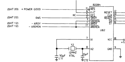 |
| The !ARDY input to the 82284 Clock Driver |
Besides handling the clock, the 82284 receives a few various READY inputs which cumulatively control the single READY line to the CPU.
With READY de-asserted until the motherboard is done with the data conversion, the 286 will idle itself via wait states, freezing any current bus operation in progress. As far as the CPU is concerned, the 16-bit transfer succeeds - it just takes a little longer to do so.
This all has an implication for 16-bit IO ports. They can only exist at even addresses. If we attempt to read or write 16-bits to an odd address, the transfer is split by the CPU, and is no longer 16 bits anymore. But an ISA card now has the choice of handling a word access to an even port address as two 8-bit ports, or one 16-bit port, depending on the status of !BHE.
This flexibility allowed certain 16-bit ISA cards to function in both AT and PC/XT systems - even with the 16-bit expansion card edge hanging in mid-air, connected to nothing.
 |
| A Oak 16-bit VGA in an 8-bit ISA slot. Yes, it works! |
Address Space Wrapping
In real mode, memory access on Intel CPUs is controlled by a system where a 16-bit segment is combined with a 16-bit offset to produce a 20-bit address. This is done by shifting the segment left by 4 bits, then adding the two values together. If this value won't fit on the bus, then it wraps around at 0.
Some software relied on this behavior, oddly enough.
IBM devised a compatibility scheme on the AT where this wrapping would be in effect by default - this was called the A20 gate, named so for the next address pin after the 8086's last address pin A19.
The A20 gate would emulate wrapping of memory around a 20-bit address bus, but could be configured to allow the entire bus in protected mode.
It is sometimes humorously observed the the A20 gate is configured on the AT's keyboard controller. This is not really as bizarre as it seems. The keyboard controller on the AT is a full microprocessor, an Intel 8042, so it is more than capable of handling a few different tasks.
The i8042 inherits the role of the PPI from the PC/XT which not only interfaced with the keyboard but was responsible for reading the DIP switches and controlling miscellaneous circuitry such as the cassette port, handling parity error signals from peripherals, etc. So sticking the A20 gate on the i8042 was not much of a leap.
Word Access and Segment Boundaries
Another interesting consideration is what happens if we read a word at the last byte address of a segment. In real mode, we are limited to reading 64KB, or offsets 0000-FFFF of the currently referenced segment. Of course if we read a word at FFFF on a 8086 or 80186, this creates an unaligned access, and so two byte transfers will be performed.
If our segment is 6000, the first byte read will be 6FFFF. This will drive BHE active, addressing the memory at 6FFFE, but with only the high byte of the bus driven to retrieve the byte at 6FFFF specifically.
But what will the next byte be? On an 8088 or 8086 CPU, the CPU's bus interface unit calculates the next offset address, which will wrap around from FFFF to 0000. The second byte read will be the first byte of the segment.
On the 80186, a word access at FFFF will calculate the next byte address by incrementing the computed address of the first byte. Since that is 6FFFF, the next byte will be at 70000, which means we read a word that straddles segment boundaries.
We can see that in action as follows:
Here is a CPU trace from an 80C86-2, reading a word with LODSW from 6000:FFFF:
000 A:[F0100:00000] M:... I:... P:..B CODE T1
001 [F0100:20100] CS M:R.. I:... P:..B CODE T2
002 [F0100:2F4AD] CS M:R.. I:... P:..B PASV T3 r-> F4AD
003 [F0100:2F4AD] CS M:... I:... P:..B PASV T4
004 A:[F0102:F0102] M:... I:... P:..B CODE T1
005 [F0102:20102] CS M:R.. I:... P:..B CODE T2
006 [F0102:29090] CS M:R.. I:... P:..B PASV T3 r-> 9090
007 [F0102:29090] CS M:... I:... P:..B PASV T4
008 [F0102:B0104] M:... I:... P:..B PASV T1
009 [F0102:B0104] M:... I:... P:..B PASV T1
010 A:[6FFFF:6FFFF] M:... I:... P:..B MEMR T1
011 [6FFFF:3FFFF] DS M:R.. I:... P:..B MEMR T2
012 [6FFFF:390FF] DS M:R.. I:... P:..B PASV T3 r-> 90
013 [6FFFF:390FF] DS M:... I:... P:..B PASV T4
014 A:[60000:60000] M:... I:... P:... MEMR T1
015 [60000:30000] DS M:R.. I:... P:... MEMR T2
016 [60000:30090] DS M:R.. I:... P:... PASV T3 r-> 90
017 [60000:30090] DS M:... I:... P:... PASV T4
And here is a CPU trace from an 80L186EB, doing the same:
000 A:[F0100:00000] M:... I:... P:..B CODE T1
001 [F0100:00100] M:R.. I:... P:..B CODE T2
002 [F0100:0F4AD] M:R.. I:... P:..B PASV T3 r-> F4AD
003 [F0100:0F4AD] M:... I:... P:..B PASV T4
004 A:[F0102:F0102] M:... I:... P:..B CODE T1
005 [F0102:00102] M:R.. I:... P:..B CODE T2
006 [F0102:09090] M:R.. I:... P:..B PASV T3 r-> 9090
007 [F0102:09090] M:... I:... P:..B PASV T4
008 [F0102:F0104] M:... I:... P:..B PASV T1
009 [F0102:F0104] M:... I:... P:..B PASV T1
010 A:[6FFFF:6FFFF] M:... I:... P:..B MEMR T1
011 [6FFFF:0FFFF] M:R.. I:... P:..B MEMR T2
012 [6FFFF:090FF] M:R.. I:... P:..B PASV T3 r-> 90
013 [6FFFF:090FF] M:... I:... P:..B PASV T4
014 A:[70000:70000] M:... I:... P:... MEMR T1
015 [70000:00000] M:R.. I:... P:... MEMR T2
016 [70000:00090] M:R.. I:... P:... PASV T3 r-> 90
017 [70000:00090] M:... I:... P:... PASV T4
Note the alignment of the bytes read within the 4-character data bus column. This illustrates a high byte (to the left, odd) vs a low byte (to the right, even).
The 286 has very different behavior than the 8086 or 80186 - an attempt to access a word at FFFF will cause an exception 13, the segment overrun exception.
Testing Emulators
An emulator author has the choice to ignore most of the exact details of an odd/even bus design, like BHE, or splitting up unaligned reads, or masking A0 to the bus. But if inherent accuracy is a goal, a set of 16-bit bus tests may be useful.
To that end, I expanded the capabilities of my
ArduinoX86 board to include 16-bit bus access and handling of the BHE pin. The cycle traces you see above were captured from this new design.
To assist in improving the accuracy of 8086 emulators, I have published a set of 8086 CPU tests that capture per-cycle bus state, including the status of the BHE line, so that you can determine if your emulator accurately reproduces the bus activity of the 8086.
Tests for the 80186 and 80286 are hopefully coming soon.
Footnotes
2) Interestingly, this "invalid" combination of A0 and BHE was later utilized by Intel in later variants of the 80186 CPU which had a DRAM refresh controller. This combination signified that a refresh cycle was being emitted by the CPU, and correspondingly, neither half of the bus should be driven.
3) Unless you had a 386SX, which was limited to a 16-bit data bus.


If the motherboard handled splitting the 16-bit unaligned memory access, how did it drive the address bus? The second byte of the transfer lives at the address + 1, so did the CLPD have an adder inside? If so, wasn't this extra slow?
ReplyDeleteA0 is not used to address the bus, so A0 ==0 and A0==1 are just 8 different wires on the same 16-bit bus address. No adder required.
DeleteI might not understand, but if A0 is not on the bus, A1 determines the 16-bit address, for _aligned_ memory access. A0 is then the even (A0=0) or the odd address (A0=1) byte. However, for _unaligned_ access, you need to first read the odd address byte of address A, but next the even address byte of address A+1. Which would need an adder.
DeleteI think we're conflating two things here - the motherboard data conversion circuit is primarily concerned with converting between 16 and 8-bit bus access. If the data conversion circuit is converting a 16-bit write to two 8-bit writes, it doesn't need to worry about alignment - that 16-bit write is guaranteed to be aligned.
DeleteTo put it another way, there is no such thing as an unaligned 16-bit write. It's physically impossible to put on the bus.
Of course, from a software perspective, we can tell the CPU to make an unaligned 16-bit write - but in that scenario, the CPU would have already converted the unaligned 16-bit write to two 8-bit writes from the start, and the data conversion circuit doesn't have to get involved.
Ah, yes, the motherboard handles 8-bit access, the CPU converts unaligned 16-bit access to two seperate 8-bit accesses. Got it now, thanks!
Delete>The next generation of Intel CPU, the 386, would come with built in support for data conversion. If the 386's BS8 pin is asserted, the CPU will use 8-bit data transfers - saving motherboard manufacturers from having to implement the data conversion logic themselves.
DeleteSadly not so :(
386 only has BS16 pin. When asserted it will internally split 32 into two 16bit cycles and additionally will output 16bit data mirrored on both halves of 32bit databus. Splitting that down to 8bit transfers is relegated to Chipset just like in 286 case you described.
486 does have BS8 pin, but its even worse than 386 because 486 doesnt mirror upper 16bit data on lower 16bit data pins. 486 will just output data on any one of its BE3–BE0 8bit banks and its again down to Chipset to redirect that particular bank to correct bus pins. Intel 486 datasheet:
"BS8# and BS16#, together with the address of data being accessed, control the sequence in which the BE0#-BE3# outputs are driven. BE0#-BE3# tell the external device which of the bytes on the full 32-bit data bus are valid in any cycle or transfer."
486 chipsets require a messy databus switchboard to accomplish this. Here how it was implemented by Maniek in his open source 486 chipset page 7 https://github.com/raszpl/M8SBC-486/blob/main/schematic_homebrew_486.pdf and vhdl logic driving it https://github.com/raszpl/M8SBC-486/blob/main/chipset/transceiver_driver.vhd
Thanks for the correction. I did most of my research with the 386EX - which does indeed have a BS8 pin as well, but that was sloppy of me not to verify as the 386EX is a very different chip from a standard 386.
Delete