Bus Sniffing the IBM 5150: Part 1
Writing a cycle-accurate emulator for a computer system is more than just understanding all the CPU instruction timings. A computer is a complete system with peripherals, interrupts, IO bus signals, and DMA. All this comes with an array of different timings and quirks.


Okay, so I've cheated a bit and skipped ahead. It took a few ground connections, and setting the appropriate voltage and filter settings in the software to get to this point where all the signals are clean. We've added a few parallel decoders to get the address bus, bus and queue status lines as well.


When software like Area 5150 is written that requires perfect cycle timing, it can be a challenge to provide the level of accuracy needed for the software to function. Area 5150 in particular requires precise coordination with the CGA's CRTC chip and timer interrupts to begin the end credits demo effect at precisely the right time. Getting this right is crucial to whether the demo effect produces this:
 |
| Artwork by VileR |
Or this:
 |
It would be very handy then if we could somehow peek into the operation of the system while it was running and understand how all these parts interact. As it turns out, we can! This process is typically referred to as 'bus sniffing', and there's a lot of a technical information out there on the topic in general. Sniffing can be done on everything from ethernet networks to vending machines, and you can even bus sniff your car. This article will specifically discuss sniffing the IBM PC 5150.
Sniffing the IBM PC is something that has been done before - I am making no claims to any great breakthroughs here. Notably, it has been done by reenigne, who designed a custom ISA card with an onboard microcontroller to capture sniffing traces. You can read about it here: https://www.reenigne.org/blog/isa-bus-sniffer-update/
Not only did he make such a neat device, he's hosted it online, so that the general public can use it. That's right - an internet connected bus sniffer, that takes your code, runs it, and responds with the cycle traces. Ingenious!
I used reenigne's bus sniffer to produce CPU cycle traces of the CPU test from 8088MPH and wrote about that here.
As cool as his bus sniffer is, it does have some limitations. Primarily, the tiny amount of memory the microcontroller has available limits it to 2048 samples. To even get the 8088MPH CPU test traces, I had to split the test up into 4 parts, changing the sample start offset each time, then reassembling the trace. Investigating something much longer - like an entire frame of a demo effect, rapidly becomes impractical. Consider that one CGA frame of 238,944 clock ticks represents 79,648 CPU cycles. That would require 39 separate sessions to accomplish, for 16.6 milliseconds of data!
I originally purchased a Siglent SDS-1104X-E 4-channel oscilloscope to investigate the composite output of the CGA card, but I have found a number of uses for it including investigating DMA timings, CGA wait states, monitoring interrupt and IO activity, among other things.
There were several times where I really wished I had more than 4 probes, and the thought naturally lead to pondering a design for my own bus sniffer. One of the main problems immediately encountered is that modern microcontrollers all run their GPIO pins at 3v, and can be damaged by the 5v signals used by the 5150.
The Arduino I used for the Arduino8088 project operates at 5V, but its slow clock rate (16MHz) and delay in switching GPIO pin directions made it unsuitable for the task of sniffing a system in realtime.
Newer microcontrollers like the Pi Pico, Teensy and Arduino GIGA are much faster - but operate at 3V, and will be damaged by 5V signals. There's some indication that the Raspberry Pi 2040 can tolerate 5v acceptably well, but no guarantees. Level shifters can be used to translate the old 5V TTL logic signals from the 5150 down to 3V for a modern microcontroller, but we would need a lot of them. They might have at most 8 lines, and we have at least 26 signals off the CPU alone. They range from either oldschool DIP packages to incredibly small surface-mount components I would barely be able to hand-solder. There are confusing warnings associated with each about speed, bidirectionality, and rumors of hard to troubleshoot glitches. I was quickly going down a rabbit hole.
Turns out I was overthinking things a bit, as long as I was willing to throw some money at the problem. There's a whole class of device designed to do exactly what I was wanting to do, without needing to build custom hardware to accomplish it.
They're called Digital Logic Analyzers. Unlike an oscilloscope, they're primarily interested in examining digital signals - and unlike a microcontroller's GPIO pins, they are tolerant of a wide range of voltage levels.
I can even add a digital logic analyzer to my Siglent scope - it's a bit of a pricey addition, $300 for the hardware and $100 for the requisite software license that unlocks the feature. In the world of digital logic analyzers, that's not too crazy, though - the top of the line Saleae Logic Pro 16 retails for a whopping $1500.
How many channels do I need, exactly? I could probably squeak by with 16, but ideally, I'd have more. Consider there are 20 address pins on the 8088 alone. Between the address/data bus, clock line, S0-S2 status lines, and QS0-QS1 status lines and other helpful signals like READY, INTR and DREQ, we're up to 28 channels already.
After some shopping around, I settled on the DSLogic U3Pro32. It offers 32 channels at 50Mhz sampling rate, USB 3.0 connectivity and decent software (based on the open source Sigrok Pulseview project).
I wasn't sure what to expect buying a "cheaper" device, but the unit that arrived seems well built (if surprisingly small) and came with a nice case for its leads.
 |
| The DSLogic U3Pro32 |
With this device I can stream the captured data directly to my PC over an arbitrary period of time, then using Python, decode the bus signals into a CPU cycle log compatible with the logs produced by MartyPC, enabling direct comparisons of cycle accuracy between hardware and emulator.
That's the theory, anyway. Now all we need is an interface.
Building the Analyzer Interface
At first blush, the task of sniffing the pins right off the 8088 might sound like a rather difficult proposition. On any other hardware platform, we might be talking about building some sort of interposer board. However the IBM PC has a very convenient feature for our purposes - a socket for an optional floating point coprocessor, the Intel 8087. In the IBM 5150, these two sockets sit side by side.

The two sockets are electrically connected on many of the same pins - shown in yellow - and they are for the most part exactly the pins we are interested in. The 20 data/address lines, the READY signal, the bus status lines S0-S2 and the queue status lines QS0-QS1. The only missing signal we really want is INTR - but we can grab that elsewhere.
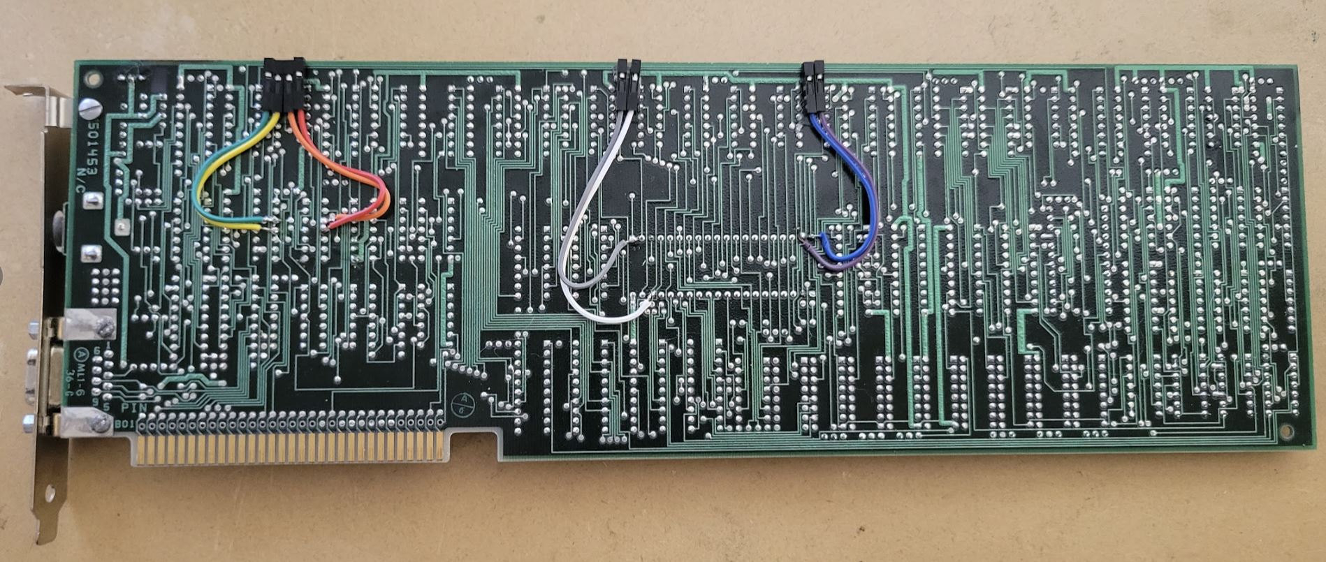
Our plan is to sniff signals directly out of the 8087 FPU socket, leaving the CPU undisturbed. Sticking 30 wires into the FPU socket is a bit impractical, so we need some sort of interface. I started thinking about designing a new PCB, but then I realized I had some Pi8088 PCBs left over from when I originally ordered them, before I built my Arduino version.
The Pi8088 is designed to have a 40 pin DIP socket attached to it and interface with the Raspberry Pi's 40 pin GPIO header. But we can repurpose it - instead of a socket, we put pins on it and it can plug into a socket instead, giving us a 40 pin header we can simply attach a standard ribbon cable to.
 |
| The NotPi8088 Socket Interface |
We don't want to connect all the CPU pins - the Pi8088 ties pin #33 to 5V to run the CPU in minimum mode - on a live system, this signal is low and the CPU is running in maximum mode. Additionally, Pin 31 is pulled to ground. So we split the pins on the status line side of the socket to leave a few disconnected. Being originally designed for an 8088 in minimum mode, the S1 and S2 pins are not connected, either. So those pins are connected with a few bodge wires.
Eventually, I plan to publish a modified PCB for this project, but for now, if you want to do the same thing you can make the same modifications.
It's not pretty, but a lot easier than designing a new PCB and waiting for it to ship from overseas - and as it turns out, it's a perfect fit, almost as if it was designed for this purpose:
 |
| 8087 Socket interface installed |
On the other end of our ribbon cable we will just use a breadboard. They make these handy 40 pin ribbon to breadboard adapters, but they're primarily designed for the Raspberry Pi GPIO lines, so getting our address lines in order takes a bit of descrambling, but eventually we have converted our FPU socket to nice neat header pins where we can attach our logic probes. Each probe has a signal and ground connection. The manual of our logic analyzer helpfully states that we can get away with a common ground connection for signals under 5Mhz, which our 4.77Mhz CPU clock is, but they were easy enough to add.
We'll utilize all 32 channels of our analyzer, which limits us to 50Mhz, but I think that will be sufficient. Here's our probe pinout:
| 0 | AD0 |
| 1 | AD1 |
| 2 | AD2 |
| 3 | AD3 |
| 4 | AD4 |
| 5 | AD5 |
| 6 | AD6 |
| 7 | AD7 |
| 8 | A8 |
| 9 | A9 |
| 10 | A10 |
| 11 | A11 |
| 12 | A12 |
| 13 | A13 |
| 14 | A14 |
| 15 | A15 |
| 16 | A16 |
| 17 | A17 |
| 18 | A18 |
| 19 | A19 |
| 20 | CLK |
| 21 | READY |
| 22 | QS0 |
| 23 | QS1 |
| 24 | S0 |
| 25 | S1 |
| 26 | S2 |
| 27 | INTR |
| 28 | DREQ |
| 29 | CLK0 |
| 30 | VSYNC (CRTC) |
| 31 | HSYNC (CRTC) |
Everything from 0-26 we can pull off the 8087 socket, the other signals will have to be routed in from miscellaneous test leads. To accomplish this, we'll use a smaller ribbon breakout:
 |
| Miscellaneous probe line interface |
This allows all our probe wires to be self contained within the PC's case; all that needs to run out are two ribbon cables.
Getting the VSYNC and HSYNC signals off the CGA is tricky. We could sniff them out of the CGA's external DB9 connector, but I'm concerned about delays between the internal CRTC logic and the card's output signals, so it's better to pull them off the CRTC chip itself:
 |
| You may want to look away. |
Probe wires are attached up to Dupont connectors for easy disconnection. If the idea of soldering probe wires to an original IBM CGA card strikes you as sacrilegious, please bear in mind that this is all reversible, and being done in the name of better understanding the system in order to preserve it for future generations. That's what I tell myself anyway to sleep better at night.
Our final internal connections look something like this:

Here's the breadboard side of things, mounted to a project board. This will be essential when we start connecting the probe wires, as they're all a bit fiddly and easily knocked about.
| GPIO breakout to breadboard interface |
Since the GPIO breakout scrambled things up, we straighten everything back out with the help of a continuity checker. I've stacked up some headers to give our probe connections a bit more clearance above the wire mess. Now we have AD0-A19 in a nice neat line, followed by our miscellaneous signals. All we need to do then, is connect our logic probe leads in order.
 |
| It isn't pretty, but it works? |
The analyzer is mounted behind onto the same project board with a command strip; this is essential to keep the probe wires from springing off on the slightest tug.
I gave up trying to attach the probe wires to the individual ground headers, instead stringing them all on a common ground like I was hanging underwear on a clothesline. Most of the probes clicked onto the headers, some were a bit loose and needed clips. There's no real clean way to do this. I did my best!
Time to see if it's all working. Let's fire up the 5150 and capture 1 second of data:
 |
| Example capture in DSView |
Okay, so I've cheated a bit and skipped ahead. It took a few ground connections, and setting the appropriate voltage and filter settings in the software to get to this point where all the signals are clean. We've added a few parallel decoders to get the address bus, bus and queue status lines as well.
DSView, and the PulseView software it is based on, supports a rather compact format which you can manipulate with a Python library, libsigrokdecode. A sensible person might have taken the time to learn how to use it, but I was impatient and didn't want to fiddle with it.
DSView can also export the data to CSV however, and what I do already know is how to process big CSV files with pandas. In "compressed" format, you basically get a row of data every time there's a change in any of the signal inputs. This still produces some enormous output files. Our 1 second capture produces a 1.4GB CSV file.
We're pretty much only interested in the low to high transition of the CPU clock, so we process our CSV file and only keep the rows that represent a low-to-high transition:
import pandas as pd
import sys

def process_chunk(chunk, prev_clk):
    chunk.columns = chunk.columns.str.strip()
    prev_clk_values = chunk['CLK'].shift(fill_value=prev_clk).astype(int)
    result = chunk[(prev_clk_values == 0) & (chunk['CLK'] == 1)]
    return result, chunk['CLK'].iat[-1]

def process_csv(input_csv, output_csv):
    prev_clk = 0
    chunk_number = 0

    with open(output_csv, 'w', newline='') as outfile:
        for chunk in pd.read_csv(input_csv, chunksize=10000, comment=';'):
            try:
                chunk_number += 1
                result_chunk, prev_clk = process_chunk(chunk, prev_clk)

                if chunk_number == 1:
                    result_chunk.to_csv(outfile, index=False)
                else:
                    result_chunk.to_csv(outfile, index=False, header=False, line_terminator='\n', mode='a')

                sys.stdout.write(f'\rProcessing chunk number {chunk_number}...')
                sys.stdout.flush()
            except Exception as e:
                print(f"An error occurred while processing chunk number {chunk_number}: {e}")

        print()

if __name__ == '__main__':
    if len(sys.argv) != 3:
        print("Usage: python export_cycles.py <input_csv> <output_csv>")
        sys.exit(1)

    input_csv, output_csv = sys.argv[1], sys.argv[2]
    process_csv(input_csv, output_csv)
This brings our CSV file down from 1.4 GB to a more manageable 338MB. As a sanity check, we can count the rows in our CSV file: 4,773,201. Fairly close to the 4,772,727 cycles we'd expect in one second.
Now comes the fun part: processing our data.
Processing the Analyzer Dump
At this point, our CSV file simply contains the values of the individual probes as they were recorded on the rising edge of each CPU clock. There are a few things we need to do; we will effectively need to emulate bits of the PC motherboard, and specifically the i8288 bus controller.
Bus States
The first thing we can do is decode the address/data bus, bus status, and queue status lines into their own columns.
One of the handy outputs of the i8288 is the ALE or "address latch enable" signal; this is a sign that the address lines of the CPU contain a valid address. The 8088 had a multiplexed address bus; at any given movement a bus pin could represent an address, data, or status bit. ALE was a signal that all the bus pins represented an address, and that it was a good time for the motherboard to latch that value if it wanted to use it later.
We can decode the S0-S2 status lines that would normally feed the i8288 ourselves; these become mnemonics such as "CODE", "MEMR", "IOW", etc. Subsequently, we don't really need to probe the ALE pin, we can detect the ALE condition when the bus mnemonic changes from the PASV condition to one of the "active" conditions.
 |
| 8088 Bus Status Lines |
This allows us to synthesize an 'ALE' column, and a corresponding 'AL' or "Address Latch" column, which repeats the value of AL as it was since the last ALE signal, until the next.
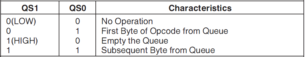
We can decode the queue status lines QS0 and QS1 into helpful characters that match MartyPC's cycle traces: an 'F' for first byte, an 'S' for subsequent byte, and an 'E' for empty/flush queue.
 |
| 8088 Queue Status Lines |
The final two status lines we want to decode are S3 and S4 which encode the active segment during an m-cycle:
 |
| 8088 Segment Status Lines |
T-States
A little trickier is calculating the T-states of the CPU. They're not exposed via any status lines, but it turns out we can figure them out with a little knowledge of how the CPU operates. We know that we begin in T1 when the ALE signal is active. We progress from T1 to T2, then to T3, which is easy enough, but at that point we have to read the READY line and insert wait states as appropriate. This requires a little state machine:
def add_t_and_d_column(df):
    state = State.TI
    next_state = None
    do_wait_state = False

    df['PREV_R'] = df['READY'].shift(1)

    for index, row in df.iterrows():

        data_bus_valid = False

        if next_state is not None:
            state = next_state
            next_state = None
        elif row['ALE'] == 'A':
            state = State.T1
        elif state == State.T1:
            state = State.T2
        elif state == State.T2:
            if row['READY'] == 1:
                data_bus_valid = True
            state = State.T3
        elif state == State.T3:
            if row['PREV_R'] == 0 or row['READY'] == 0:
                state = State.Tw
            else:
                state = State.T4
        elif state == State.Tw:
            if row['PREV_R'] == 1:
                data_bus_valid = True
                state = State.T4
            else:
                state = State.Tw
        elif state == State.T4:
            state = State.TI

        if data_bus_valid
            df.at[index, 'D'] = decode_data(row)

        # Set the T column for the current row
        df.at[index, 'T'] = state.name

    # Drop the temporary column after use
    df = df.drop(columns=['PREV_R'])

    return df
While we're calculating T states, we might as well read the data bus at the appropriate time - either T3, or the last Tw state - which we do with the call to decode_data(), putting the value in a 'D' column.
Queue Status and Contents
We have all the information we need to keep track of the CPU's instruction queue, as well. If our bus status is CODE, we put any bytes in the 'D' column into the queue - which we represent with four additional columns, Q0-Q3. If our queue status column QOP indicates a queue byte is read, we pull that byte back out of the queue, and append it to an INST column. This column builds up the hexadecimal representation of the instruction being executed.
We can print some warnings to the console it looks like the CPU is reading from an empty queue, or writing to a full one. This is a good sanity check against our data.
If we happen to flush the instruction queue, we can accordingly clear the Q0-Q3 columns as well.
We can determine when instructions begin and end by the queue status of 'F' or 'first byte' - this signals an instruction is beginning, and by extension, the previous instruction is ending. At that point, we can take the hexadecimal string contained in INST and disassemble it.
I didn't want to try to port MartyPC's disassembler to Python, but thankfully I didn't have to, disassembling is as easy as importing iced-x86 and letting iced do all the grunt work.
def disassemble(df):

    bitness = 16  # 16-bit for 8088

    for index, row in df.iterrows():
        inst_hex = row['INSTF']
        if inst_hex and not pd.isna(inst_hex):
            try:
                inst_bytes = bytes.fromhex(inst_hex)

                decoder = Decoder(bitness, inst_bytes)
                for instr in decoder:
                    # Create a formatter and get the disassembled instruction
                    formatter = Formatter(FormatterSyntax.NASM)
                    disassembled = formatter.format(instr)

                    # Assign the disassembled instruction to a new column in the DataFrame
                    df.at[index, 'DISASM'] = disassembled
            except Exception as e:
                print(f"Error disassembling instruction at index {index}: {e}")
                continue

    return df
Here's what our decoded cycle data looks like:
| ALE | AL | SEG | BUSL | READY | T | D | QOP | QB | INSTF | DISASM | QL | Q0 | Q1 | Q2 | Q3 | QS0 | QS1 | S0 | S1 | S2 | CLK0 | INTR | DR0 | VS | HS |
| . | PASV | 1 | TI | . | 0 | 0 | 0 | 1 | 1 | 1 | 1 | 1 | 0 | 0 | 0 | ||||||||||
| . | PASV | 1 | TI | . | 0 | 0 | 0 | 1 | 1 | 1 | 0 | 1 | 0 | 0 | 0 | ||||||||||
| A | '14740 | CODE | 1 | T1 | . | 0 | 0 | 0 | 0 | 0 | 1 | 0 | 1 | 1 | 0 | 0 | |||||||||
| . | '14740 | CS | CODE | 1 | T2 | S | 0 | 1 | 1 | 0 | 0 | 1 | 1 | 1 | 1 | 0 | 0 | ||||||||
| . | '14740 | CS | CODE | 1 | T3 | 'EC | . | 1 | 'EC | 0 | 0 | 1 | 1 | 1 | 1 | 1 | 1 | 0 | 0 | ||||||
| . | '14740 | CS | CODE | 1 | T4 | . | 1 | 'EC | 0 | 0 | 1 | 1 | 1 | 0 | 1 | 1 | 0 | 0 | |||||||
| . | '14740 | PASV | 1 | TI | . | 1 | 'EC | 0 | 0 | 1 | 1 | 1 | 0 | 1 | 1 | 0 | 0 | ||||||||
| . | '14740 | PASV | 0 | TI | . | 1 | 'EC | 0 | 0 | 1 | 1 | 1 | 1 | 1 | 1 | 0 | 0 | ||||||||
| . | '14740 | PASV | 0 | TI | . | 1 | 'EC | 0 | 0 | 1 | 1 | 1 | 1 | 1 | 0 | 0 | 0 | ||||||||
| . | '14740 | PASV | 0 | TI | . | 0 | 0 | 0 | 1 | 1 | 1 | 0 | 1 | 0 | 0 | 0 | |||||||||
| . | '14740 | PASV | 0 | TI | E | 0 | 0 | 1 | 1 | 1 | 1 | 0 | 1 | 0 | 0 | 0 | |||||||||
| . | '14740 | PASV | 0 | TI | . | 0 | 0 | 0 | 1 | 1 | 1 | 1 | 1 | 0 | 0 | 0 | |||||||||
| A | '1473B | CODE | 0 | T1 | . | 0 | 0 | 0 | 0 | 0 | 1 | 1 | 1 | 0 | 0 | 0 | |||||||||
| . | '1473B | CS | CODE | 1 | T2 | . | 0 | 0 | 0 | 0 | 0 | 1 | 0 | 1 | 0 | 0 | 0 | ||||||||
| . | '1473B | CS | CODE | 1 | T3 | 'EC | . | 1 | 'EC | 0 | 0 | 1 | 1 | 1 | 0 | 1 | 0 | 0 | 0 | ||||||
| . | '1473B | CS | CODE | 1 | T4 | . | 1 | 'EC | 0 | 0 | 1 | 1 | 1 | 1 | 1 | 0 | 0 | 0 | |||||||
| A | '1473C | CODE | 1 | T1 | . | 'EC | ' | 0 | 0 | 0 | 0 | 0 | 1 | 1 | 1 | 0 | 0 | 0 | |||||||
| . | '1473C | CS | CODE | 1 | T2 | F | in al,dx | 0 | 1 | 0 | 0 | 0 | 1 | 0 | 1 | 0 | 0 | 0 | |||||||
| . | '1473C | CS | CODE | 1 | T3 | 'A8 | . | 1 | 'A8 | 0 | 0 | 1 | 1 | 1 | 0 | 1 | 0 | 0 | 0 | ||||||
| . | '1473C | CS | CODE | 1 | T4 | . | 1 | 'A8 | 0 | 0 | 1 | 1 | 1 | 1 | 1 | 0 | 0 | 0 | |||||||
| . | '1473C | PASV | 1 | TI | . | 1 | 'A8 | 0 | 0 | 1 | 1 | 1 | 1 | 1 | 0 | 0 | 0 | ||||||||
| . | '1473C | PASV | 1 | TI | . | 1 | 'A8 | 0 | 0 | 1 | 1 | 1 | 0 | 1 | 0 | 0 | 0 | ||||||||
| A | '003DA | IOR | 1 | T1 | . | 1 | 'A8 | 0 | 0 | 1 | 0 | 0 | 0 | 1 | 0 | 0 | 0 | ||||||||
| . | '003DA | CS | IOR | 1 | T2 | . | 1 | 'A8 | 0 | 0 | 1 | 0 | 0 | 1 | 1 | 0 | 0 | 0 | |||||||
| . | '003DA | CS | IOR | 0 | T3 | . | 1 | 'A8 | 0 | 0 | 1 | 0 | 0 | 1 | 1 | 0 | 0 | 0 | |||||||
| . | '003DA | CS | IOR | 1 | Tw | . | 1 | 'A8 | 0 | 0 | 1 | 1 | 1 | 0 | 1 | 0 | 0 | 0 | |||||||
| . | '003DA | CS | IOR | 1 | T4 | 'F7 | . | 'A8 | 'EC | 0 | 0 | 0 | 1 | 1 | 1 | 0 | 1 | 0 | 0 | 0 | |||||
| A | '1473D | CODE | 1 | T1 | F | test al,1 | 0 | 1 | 0 | 0 | 0 | 1 | 1 | 1 | 0 | 0 | 0 | ||||||||
| . | '1473D | CS | CODE | 1 | T2 | . | 0 | 0 | 0 | 0 | 0 | 1 | 1 | 1 | 0 | 0 | 0 | ||||||||
| . | '1473D | CS | CODE | 1 | T3 | '01 | . | 1 | '01 | 0 | 0 | 1 | 1 | 1 | 0 | 1 | 0 | 0 | 0 | ||||||
| . | '1473D | CS | CODE | 1 | T4 | . | 1 | '01 | 0 | 0 | 1 | 1 | 1 | 0 | 1 | 0 | 0 | 0 | |||||||
| A | '1473E | CODE | 1 | T1 | . | '01 | 0 | 0 | 0 | 0 | 0 | 1 | 1 | 1 | 0 | 0 | 0 | ||||||||
| . | '1473E | CS | CODE | 1 | T2 | S | 0 | 1 | 1 | 0 | 0 | 1 | 1 | 1 | 0 | 0 | 0 |
This might appear to be mostly Greek, but all the relevant information has been decoded. The real important stuff is 'D' - the contents of the data bus during a read or write, and 'DISASM' which is our instruction disassembly, conveniently placed on the first cycle of each instruction.
Making it Pretty - Excelify.py
Pouring through thousands of lines of text can be pretty tedious, and spotting certain details difficult. It would be nice if we could use some formatting to make certain information 'pop' more. What if we could delineate the boundaries between instructions, for example?
It's surprisingly easy to create and manipulate Excel files with Python using the openpyxl library. We can load our CSV file, convert it to Excel, and then crunch on it. Adding a thick, top border at the start of all instructions is easy - when the column 'DISASM' contains a value, we iterate through all cells in that row and draw a thick top border on each.
While we're at it, we can create a mapping of how to set the fill color for certain cells:
COLOR_MAP = {
    'SEG': {
        #'CS': LIGHT_BLUE,
        'DS': PASTEL_GREEN,
        'SS': PASTEL_PINK,
        'ES': PASTEL_YELLOW
    },
    'T': {
        'TI': LIGHT_GRAY,
        'Tw': LIGHT_BLUE
    },
    'QOP': {
        'F': PASTEL_MINT,
        'S': PASTEL_YELLOW,
        'E': PASTEL_PINK,
    }
}
We can get even fancier, too. The digital analyzer shows us a visual representation of our clock lines - can we replicate that? Turns out, we can. If we identify certain columns we want to interpret visually, we can add two columns to the right of each, and draw a clock signal using cell borders and fill.
Here's what the result looks like:

READY (the pastel blue column) isn't a clock, but it's interesting to see it visualized - it makes it easy at a glance to see the relationship between the READY status and wait states (which are now also highlighted blue). The pink line is our CLK0 signal - the clock line that drives the 8253 timer chip; this is useful for lining up exactly when our reload values get set after an OUT instruction reprograms a timer channel, since that is triggered by the falling edge of the timer clock.
Where this is really useful is when you zoom out:

If you're scanning along looking for an interrupt, this is a lot harder to miss. Now we can see our DMA requests in light cyan as well as a full HSYNC period in lavender.
Note that we're not just decoding VSYNC and HSYNC; we're counting elapsed frames (incremented when VSYNC transitions low) and calculating the effective raster position within the NTSC field, which should come in handy.
There's a lot we can do with a spreadsheet format; we can add additional worksheets, such as a list of all instructions and cycle counts, with links back to their position in the cycle trace:
 |
| Instruction Index Sheet |
We can do the same for IO operations, as well. We can even use an external lookup file to provide a human-readable port description (data from Bochs' PORTS.LST):
 |
| IO Operation Index Sheet |
Since we can have formulas, charts, VLOOKUPS and such, (and as of recently, even Python) there are quite a lot of interesting things we can potentially do. Don't worry, most of this all works fine in Google Sheets or LibreOffice Calc as well. I will be publishing cycle traces in ODF format. I would have done everything natively within ODF, but surprisingly, the Python libraries for manipulating Excel documents are far more mature.
The main limitation here is that Excel is limited to 1 million rows. At 4.77 MHz, that limits our usable formatted traces to a quarter of a second. Still, 1 million cycles is a lot when we've been used to only 2048!
So Now What?
Now that we can get cycle traces off the IBM 5150, we can use them to deep-dive into certain situations, like say, the beginning of Area 5150's end credits effect, which is a rather complicated bit of code and device coordination.
Waiting for the end of Area 5150 for the credit sequence to begin would be abysmally tedious - and trying to capture the very first second of it nearly impossible - so I decompressed the Area 5150 loader and modified the execution script within it to produce an executable that skips right to the end credit effect directly. I named this file 'acredits.com'. Now we just need a way to coordinate our trace capture with program execution.
As it turns out, we can use any of our probe inputs as a capture trigger. INTR is a decent candidate. Sitting at a DOS prompt, there's really only one kind of interrupt going on - the regular timer interrupt. We can turn this off, either via stopping Timer channel #0, or masking IRQ0 on the PIC - we'll do the latter with a short utility I call 'stoptime.com':
With timer interrupts disabled, we can type out our command 'acredits.com' and then arm our logic analyzer to trigger on the INTR line, which should begin capture on the next interrupt that occurs. Since we've disabled timer interrupts, the next interrupt should happen when we hit the enter key and generate an IRQ2.
Let's try it out:

The red marker indicates the trigger point. We get about 50ms of data before the trigger. This is fine - it's still probably better than trying to click start in the analyzer software and press enter on the 5150 at the same time.
There are of course other potential ways to trigger a capture. We could use an ISA breadboard kit like the one sold by TexElec to respond to a specific port address - maybe even an existing one, if we're careful to simply listen in. This could potentially allow all sorts of fancy triggers - imagine triggering a capture on a specific timer reload value or CRTC register write. The options there are really endless, especially if you add a microcontroller of some kind. If you use a custom trigger, however, you'll be giving up one of your probe lines.
What we're really interested in with this trace in particular is investigating the initial interrupt chain that sets up the "vsync" ISR the effect uses to draw. If we scan a bit ahead in our capture, we can locate where the Lake effect ISR setup begins:

Watch the VS line - we can see a series of short CRTC frames used in the timing setup; corresponding to some frenetic interrupt activity. The final result and end goal is seen in the last two VSYNCs on the right - a nice, consistent interrupt at a consistent point after VSYNC. Note that it is not immediately after VSYNC, instead it is delayed to just before the start of display enable. The main Lake effect will run like this until termination without further interrupt tricks.
To Be Continued...
Ok, so this is a bit of a tease - but this article is a bit long as it is, and actually using our new cycle trace powers to debug Area 5150 will be a long topic by itself, best left for a follow-up article or two.
If you're interested in replicating this yourself, here are the following links you may need:
U3Pro32 Logic Analyzer (non-affiliate link)
If you have some ideas or requests for cycle traces, please respond to this thread on VOGONS.
Thanks for reading!


Comments
Post a Comment